Technology
Author: Jeff W. Hockert, Senior Marketing Manager at Intel
As electrical interconnects face performance barriers and data centers confront a power wall, Intel is advancing its vision of Integrated Photonics. By transmitting data optically, at lower latencies, higher bandwidth, and much lower power than is possible with electrical connections, Intel believes Integrated Photonics will fundamentally change data center architectures.
Intel’s Silicon Photonics vision began in 2004 with a goal of pulling together the optical and electronic functions into one chip. A lot of progress has been made since then. For example, there are now over 4 million Intel 100G optical transceivers being used for rack-to-rack connectivity — connecting row switches and director-class switches throughout data centers.
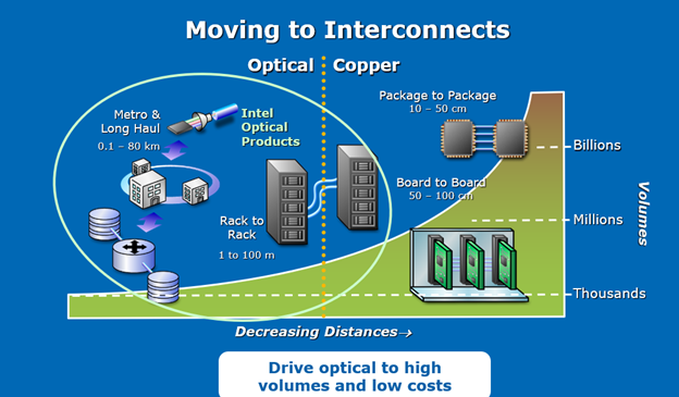
Today, optical interconnects over fiber dominate long-distance interconnects, while electrical dominates short distances. Our goal is to advance optical performance and replace electrical by bringing optical I/O directly into servers for board-to-board and package-to-package connectivity.
And the need is there: current I/O performance of electrical interconnects are running into practical performance limits. Equally important, data centers are faced with power-consumption challenges. Bandwidth demand for compute approximately doubles every two years¹. However, electrical performance-scaling is not keeping pace with bandwidth demand. Moreover, electrical I/O energy efficiency has slowed recently, resulting in an approaching power wall. Specifically, the I/O power is trending to be larger than the total available socket power, leaving nothing for compute.
In traditional server systems, scaling electrical interconnect requires higher data rates and adding more I/O pins, which increases the package size to meet bandwidth demand. However, this doesn’t solve the power wall. Without fundamental breakthroughs, these two trends will not change over time. Optical I/O has the potential to be more efficient than electrical I/O while simultaneously providing >1000 times more reach². By tightly integrating optical into a server package using silicon photonics, we can gain three benefits in a smaller footprint: (1) lower power (2) higher bandwidth and (3) reduced pin count.

We call this research vision Integrated Photonics and believe it will fundamentally change our data center network architectures. It will free data to move around the data center much more efficiently — at both lower power and lower latency. Our research goals are 1Tb/s per fiber at @ 1pJ/b with up to a 1km reach. By reducing the optical I/O power below electrical I/O and miniaturizing the footprint of our silicon photonics devices to drive down cost, we are confident we can address the approaching I/O power wall.
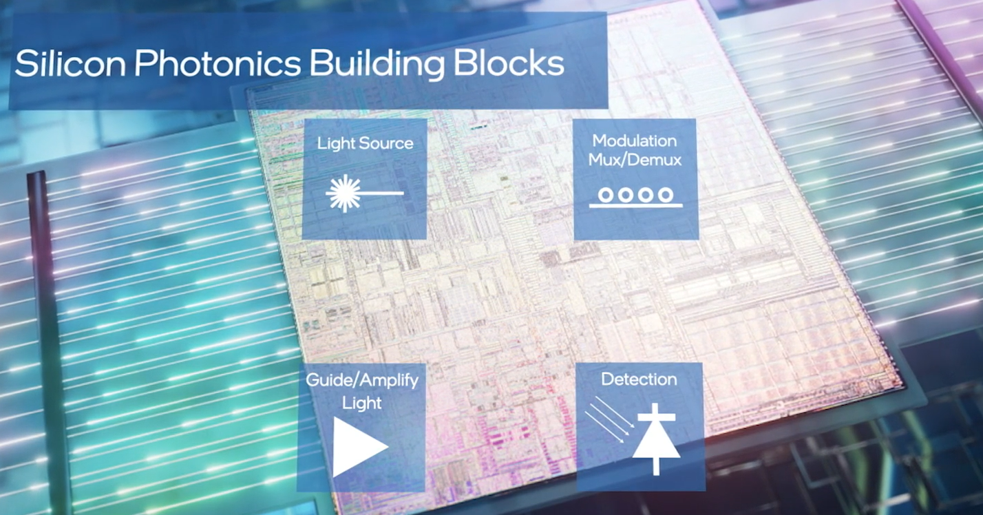
Let’s drill down and see what technologies are needed to achieve Intel’s vision of connecting data centers with light. At Intel Labs Day 2020, held on Dec. 3rd, Intel showed photonics ICs with fully integrated photonics functions, including the laser, amplifier, and ring modulators/detectors. We showed breakthrough advances in (1) micro-ring modulators, (2) an all-silicon photodetector, (3) optical amplifiers integrated with the lasers and (4) CMOS circuit integration.
We have developed micro-ring modulators which are a thousand times smaller than conventional silicon modulators. The micro rings serve as a light modulator, and as a silicon photodetector. Until now, the industry believed that silicon had virtually no light detection capability in the 1.3–1.6um wavelength range, seen as a fundamental limitation for silicon photonics technology. That was proved wrong. On the receiver side, we have been working on all silicon ring-based photodetectors which combine wavelength selection and photodetection functions in a single device. Earlier this year we published light detection capability with an all-silicon photodetector, and demonstrated this photodetector operating at a data rate of 112Gb/s.
These ring photodetectors can be assembled with CMOS trans-impedance amplifiers to build low-cost optical receivers. A major advantage of this approach is processing and material cost reduction.
We have integrated multi-wavelength lasers. We showed a 4-wavelength laser which uses a single cavity, making it a more compact laser with uniform channel spacing. Semiconductor optical amplifiers are another indispensable technology. It is challenging to generate all the required light power from a laser. Fortunately, Intel’s optical amplifiers can be more power efficient, and it is important to note that they are made from the same material used for the integrated laser. Without the integrated laser, these amplifiers are not possible.
Finally, the co-integration of CMOS circuitry and silicon photonics brings all these technologies together. Early this year we described our ability to 3D stack the CMOS electronic IC with our photonics IC using copper pillars. The CMOS electronic IC includes interface circuits to transmit, receive, and thermally control the ring modulator to track temperature variations.
By directly stacking the two ICs, one on top of the other, we demonstrated the real potential of micro-rings and CMOS circuitry being integrated together. The die-to-die integration results in a 3D-integrated 100G silicon photonic transmitter, capable of signaling at 112 Gbps.
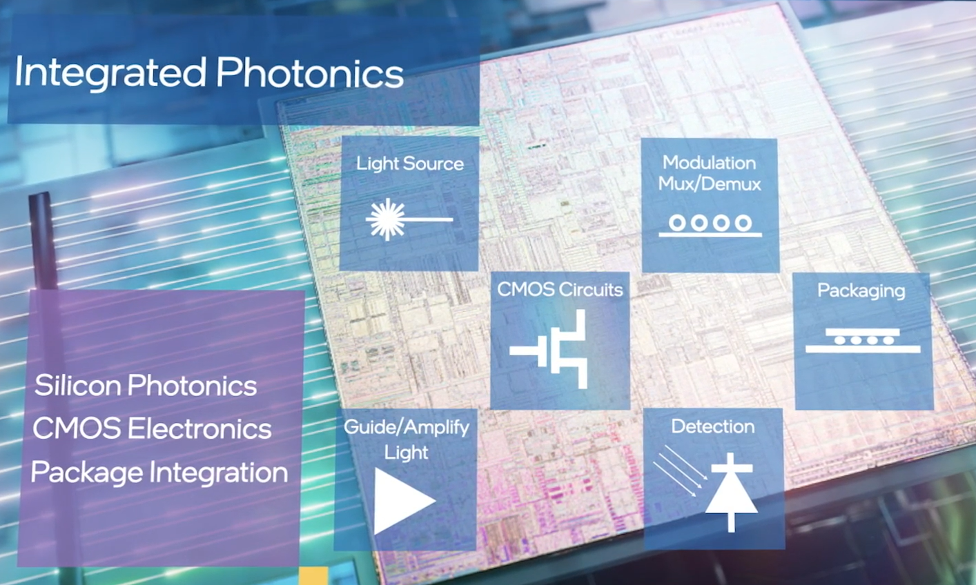
With excellent package integration technology developed by Intel’s packaging group, we have a path to integrate the most advanced CMOS technology and silicon photonics for bringing products with unmatched interconnect performance to our customers. Intel is unique in its ability to deliver integrated multi-wavelength lasers, semi-conductor optical amplifiers, all-silicon photodetectors, and micro-ring modulators on a single silicon technology platform, along with the technology to tightly integrate them with CMOS silicon.
Integrating photonics onto a package for servers is not a new idea. The key difference is that we now have all the required technologies on a single silicon photonics platform to make this vison a reality. With our micro-ring modulators being reduced to just microns in size, we can integrate 100s of optical I/O in a small footprint. We believe these types of optical links demonstrated at Intel Labs Day 2020 can be scaled to enable bandwidths of 10s to 100s of terabits per second, and will increase optical I/O volumes from millions today to billions of units, driving down manufacturing costs.
About the Author
Jeff Hockert is a senior marketing manager in the Technology Leadership Marketing (TLM) team at Intel.
Notices and Disclaimers
¹ Source(s):
² Source:
Performance varies by use, configuration and other factors. Learn more at www.Intel.com/PerformanceIndex.
Intel technologies may require enabled hardware, software or service activation. No product or component can be absolutely secure.
© Intel Corporation. Intel, the Intel logo, and other Intel marks are trademarks of Intel Corporation or its subsidiaries. Other names and brands may be claimed as the property of others.
"light" - Google News
May 11, 2021 at 07:37AM
https://ift.tt/3eCe5kU
Integrated Photonics Set to Light Up the Data Center - Medium
"light" - Google News
https://ift.tt/2Wm8QLw
https://ift.tt/2Stbv5k
Bagikan Berita Ini


0 Response to "Integrated Photonics Set to Light Up the Data Center - Medium"
Post a Comment