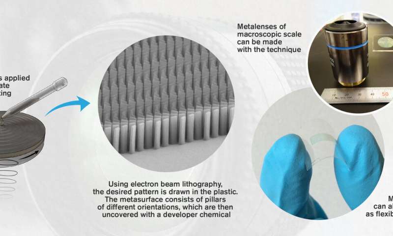
In the future, camera lenses could be thousands of times thinner and significantly less resource-intensive to manufacture. Researchers from Chalmers University of Technology, Sweden, now present a new technology for making artificial materials known as metasurfaces, which consist of a multitude of interacting nanoparticles that, together, can control light. They could have great use in the optical technology of tomorrow.
Metasurfaces can be used for optical components in portable electronics, sensors, cameras or space satellites. The Chalmers researchers' new technology for making such planar surfaces is based on a plastic that is already used today to create other microstructures.
"We put a thin layer of this plastic on a glass plate and, using a well-established technique called electron-beam lithography, we can draw detailed patterns in the plastic film, which, after development, will form the metasurface. The resulting device can focus light just like a normal camera lens, but it is thousands of times thinner—and can be flexible too," says Daniel Andrén, a Ph.D. student at the Department of Physics at Chalmers and first author of the scientific article recently published in the journal ACS Photonics.
Over the past 10 years, there has been a revolution in optics. Smartphones have cameras comparable to a DSLR, with millions of pixels of resolution. They process light with small, advanced computer chips and software, and the image is recreated with the help of small colored LEDs. These technologies have developed extremely rapidly in recent years, due mainly to smaller and more effective circuit components.
However, camera lenses themselves have not changed as much. The majority of today's lenses are based on the same physical principles, and include the same basic limitations as the first prototypes invented in the 16th century. In the past decade, however, researchers have begun to work with artificial materials—metasurfaces—that could replace today's lenses.
Currently, certain issues stand in the way of the large-scale manufacturing of metasurfaces. Advanced equipment is required to manufacture them, and the process is time-consuming. But using the Chalmers researchers' new method, the production rate can be increased several times compared to current state-of-the-art techniques. The new technology uses harmless chemicals, as well as machines that are already common in nano-manufacturing laboratories today, meaning that more researchers could now begin to study metasurfaces.
"Our method could be a step toward large-scale production of metasurfaces. That is the goal we are already working toward today. Metasurfaces can help us create different effects and offer various technological possibilities. The best is yet to come," says Ruggero Verre, a researcher at the Department of Physics at Chalmers and co-author of the scientific article.
Explore further
Citation: Ultra-thin camera lenses of the future could see the light of day (2020, June 11) retrieved 11 June 2020 from https://ift.tt/3hkJg3e
This document is subject to copyright. Apart from any fair dealing for the purpose of private study or research, no part may be reproduced without the written permission. The content is provided for information purposes only.
"light" - Google News
June 11, 2020 at 06:45PM
https://ift.tt/3hkJg3e
Ultra-thin camera lenses of the future could see the light of day - Phys.org
"light" - Google News
https://ift.tt/2Wm8QLw
https://ift.tt/2Stbv5k
Bagikan Berita Ini


0 Response to "Ultra-thin camera lenses of the future could see the light of day - Phys.org"
Post a Comment