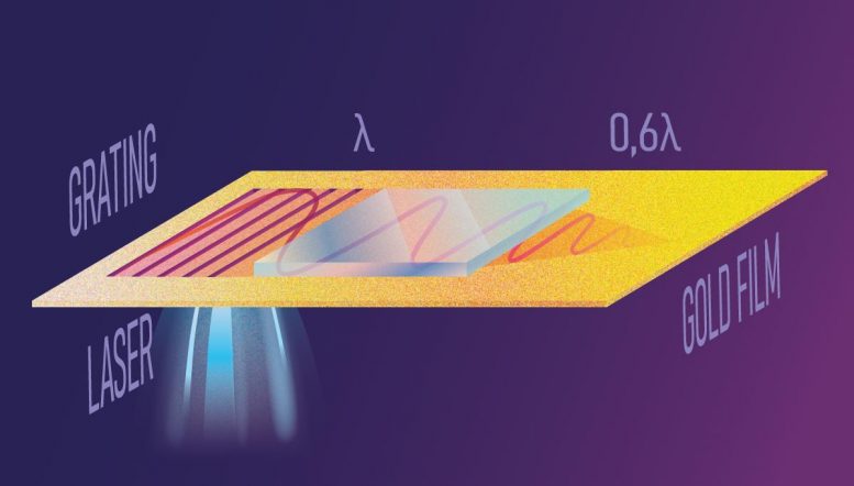
An artist’s conception of the superlens compressing a laser beam into more manageable, lower-wavelength electromagnetic oscillations. Scroll down for a more accurate graphic representation. Credit: Daria Sokol/MIPT Press Office
Plasmon nanojet: Physicists implement efficient mechanism for subwavelength focusing of plasmons.
Russian and Danish researchers have made a first-ever experimental observation of a plasmon nanojet. This physical phenomenon enables nanoscale focusing of light and, theoretically, allows engineers to bypass one of the fundamental limitations of the ordinary converging lens. Tight compression of light waves is necessary to use them as signal carriers in compact devices that would work much faster than today’s electronics. The study was published in the June 15, 2020, issue of Optics Letters.
Before laser pointers became available, the amorous heroes of romance novels had to make do with small rocks they would throw into a beloved’s window to indicate their presence. Among the numerous drawbacks of rocks as signal carriers is their mass, which means sending a message requires an effort and time. While the electron does not weigh as much as a rock, it still cannot be put in motion instantaneously. If we could replace the electrons in microcircuits with photons — the massless particles of light — the resulting devices would operate much faster.

Plasmon nanojet-based superlens. When a laser pulse of wavelength λ shines on the diffraction grating in the gold film, this gives rise to another type of electromagnetic excitations, known as surface plasmon polaritons. They propagate along the gold film and undergo 60% compression to a wavelength of 0.6λ when passing the square nanoparticle. This so-called plasmon nanojet effect, observed in the study for the first time, offers intriguing prospects for localizing light to the point where it becomes feasible to use it in fast and compact optical computers. Credit: Daria Sokol/MIPT Press Office
What prevents engineers from abandoning electronic chips in favor of their photonic analogs is the need for miniaturization. With today’s technology, such optical devices would have an enormous size. To make them smaller, engineers require a way to control photons on such a small scale that the light wave itself has to be localized, squeezed into a minimum space. Ideally, the light needs to be focused into a spot smaller than 50% of the original wavelength. While this feat is impossible in the classical optics due to what’s known as the diffraction limit, modern research has already found several ways around it. And the newly observed plasmon nanojet is likely to become one of them.
A team of Russian and Danish physicists has created a focusing component, or nanolens, capable of converting light into electromagnetic waves of a special kind, compressing it to 60% of the initial radiation wavelength. This new contraption is made up of a square piece of dielectric material 5 by 5 micrometers in size and 0.25 micrometers thick. Shown in figure 1, the square particle lies on a thin 0.1-micrometer gold film, next to an etched grating that diffracts light.

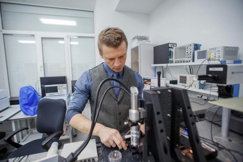
Paper co-author Valentyn Volkov is working with a near-field microscope. A device of this kind was used in the study to make the first-ever observation of a plasmon nanojet. Credit: Evgeniy Pelevin/MIPT Press Office
Illuminating the grating in the gold film with a laser generates excitations known as surface plasmon polaritons, which travel along the metal’s surface. These SPPs are essentially two kinds of waves coupled to each other and propagating together. First, there’s the collective oscillation of electrons in gold — the plasmon part — and then there’s also a surface light wave called a polariton. The point of converting light to SPPs is that there are ways to focus them to a greater extent than the initial laser pulse.
“One of the mechanisms that enable subwavelength focusing relies on the plasmon nanojet, a phenomenon we have observed in an experiment for the first time,” said the paper’s lead author, Professor Igor Minin of Tomsk Polytechnic University.
The scientific explanation of why waves undergo compression in the superlens is as follows. “Using computer simulations, we figured out the appropriate dimensions of the dielectric particle and the diffraction grid in the gold film. When these parameters are right, SPPs have different phase velocities at different points in the particle. This causes the wavefront to bend, creating a vortex in the particle and therefore a region dense with SPPs behind it, which we call a plasmon nanojet,” said study co-author Dmitry Ponomarev, a leading researcher at the MIPT Laboratory of 2D Materials and Nanodevices and the deputy director of Mokerov Institute of Ultra High Frequency Semiconductor Electronics of the Russian Academy of Sciences.
The study has demonstrated a new and efficient mechanism for strongly localizing radiation and manipulating it on the nanoscale, which is a prerequisite for densely packing optical components in photonic and plasmonic devices that would operate much faster than conventional electronics.
The head of the MIPT Center for Photonics and 2D Materials, Valentyn Volkov, who co-authored the study, added: “The experimental observation of plasmon nanojets has been made possible by a concerted effort on the part of our center’s researchers and the colleagues in Moscow, Tomsk, and Copenhagen. This collaboration is not over, and we are planning to show other exciting effects that have to do with the formation, propagation, and application of plasmon nanojets.”
Reference: “Plasmonic nanojet: an experimental demonstration” by Igor V. Minin, Oleg V. Minin, Igor A. Glinskiy, Rustam A. Khabibulin, Radu Malureanu, Andrei V. Lavrinenko, Dmitry I. Yakubovsky, Aleksey V. Arsenin, Valentyn S. Volkov and Dmitry S. Ponomarev, 9 June 2020, Optics Letters.
DOI: 10.1364/OL.391861
"light" - Google News
June 19, 2020 at 06:48AM
https://ift.tt/37G05Bv
Plasmon Nanojet: Superlens Squeezes Light Into Nanospace - SciTechDaily
"light" - Google News
https://ift.tt/2Wm8QLw
https://ift.tt/2Stbv5k
Bagikan Berita Ini


0 Response to "Plasmon Nanojet: Superlens Squeezes Light Into Nanospace - SciTechDaily"
Post a Comment