ROCHESTER, N.Y., Nov. 5, 2020 — Using magnetic and semiconducting materials, researchers at the University of Rochester and Cornell University designed a nanoscale node capable of using laser light to emit and accept photons to interact with other nodes. Compared to current networks used to perform computations and communications, the quantum mechanics development capitalizes on light’s physical properties to deliver a faster, increasingly efficient method to perform computations and detections involving objects and materials.
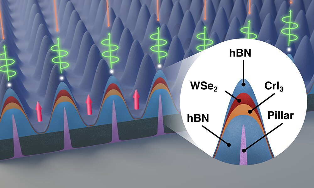
In the design, the researchers arranged semiconductor and magnetic materials to form a platform that consisted of an array of pillars, each 120 nm in height. The pillars mark the location of a distinct quantum state that can interact with photons, and allow the photons to come into contact with other locations across the device and with similarly constructed arrays at various locations. A distinctive alignment of tungsten diselenide (WSe2) is draped over the pillars with a highly reactive layer of chromium triiodide (Crl3),
At the point where atomically thin, 12-µm-area layers touch (the design expands on previous work the Vamivakas Lab introduced, which used WSe2 placed in Van der Waals heterostructures to create or capture single photons using layers of atomically thin materials placed on top of one another), the Crl3 electrically charges the WSe2. This creates a physical characteristic that resembles a hole alongside the base of each pillar.
In quantum physics, the absence of an electron characterizes a hole; each positively charged hole also possesses a binary north/south magnetic property.

A closeup of an array of pillars, each 120 nm high. Each pillar serves as a location marker for a quantum state that can interact with photons. A novel alignment of tungsten diselenide (WSe2) is draped over the pillars with an underlying, highly reactive layer of chromium triiodide (CrI3). Where the atomically thin, 12-µm-area layers touch, the CrI3 imparts an electric charge to the WSe2, creating a 'hole' alongside each of the pillars. Courtesy of the University of Rochester (illustration) via Michael Osadciw.
Given that quality, each hole is also a nanomagnet. When the researchers shined laser light over the entire device, those nanomagnets turned into optically active spin areas, which, as a result, also emitted and interacted with photons. Spin states, as opposed to bits used in traditional information processing that have values of 0 or 1, can encode both values at the same time and increase the possibilities for information processing.
Due to the properties and concept of entanglement, the system established the potential for quantum nodes to connect across a fully remote network. The system functions like a register, in which information can be stored at different spatial locations that interact with photons, said Nick Vamivakas, professor of quantum optics and quantum physics at the University of Rochester. The dynamic supports a move toward the development of a functional communications network that uses photons to distribute acquired information across long distances.
Further, controlling the spin orientation with ultrathin and appropriately sized (120 µm) Crl3 components eliminates the need for external magnetic fields. Because the magnetic coils used to deliver such fields are so large (the researchers said the same types of coils are used in MRI systems), the method of control the researchers used supports miniaturizing a quantum computing device, based on single hole spins, said Arunabh Mukherjee, lead author of study describing the advance.
The Rochester-based team collaborated with Cornell researchers to create the necessary inert environment in which the researchers could most effectively work with Crl3, given its highly reactive nature. The collaborators ultimately fabricated Crl3 in glove boxes filled with nitrogen to avoid degradation caused by oxygen and moisture.
Another challenge is optimizing the configuration of pillars to ensure that each corresponding hole and spin valley can be properly assigned (registered) to eventually link to other nodes across the device. In broad terms, the researchers must find a way to send photons over long distances, through an optical fiber, to other nodes, without compromising entanglement or photonic properties.
That work is forthcoming, Vamivakas said. Vamivakas and Mukherjee were joined on the paper describing the work by coauthors Kamran Shayan, of Vamivakas’ lab, as well as Lizhong Li, Jie Shan, and Kin Fai Mak from Cornell.
The research was published in Nature Communications (www.doi.org/10.1038/s41467-020-19262-2).
"light" - Google News
November 05, 2020 at 07:03PM
https://ift.tt/362KSKi
Light-Driven Quantum Network Promises Faster, Enhanced Communication - Photonics.com
"light" - Google News
https://ift.tt/2Wm8QLw
https://ift.tt/2Stbv5k
Bagikan Berita Ini


0 Response to "Light-Driven Quantum Network Promises Faster, Enhanced Communication - Photonics.com"
Post a Comment